Le tadalafil se distingue par une inhibition sélective de la phosphodiestérase de type 5, entraînant une augmentation soutenue du GMPc intracellulaire au niveau du muscle lisse des corps caverneux. Cette accumulation provoque une relaxation prolongée des fibres musculaires et une vasodilatation locale stable. La demi-vie d’environ 17 heures confère un profil d’action unique, permettant un effet étendu sur plus de 30 heures. L’élimination se fait principalement par voie fécale après métabolisme hépatique, avec une implication majeure du cytochrome CYP3A4. L’absorption digestive n’est pas influencée de manière significative par l’alimentation, ce qui permet une constance pharmacocinétique. La mention cialis sans ordonnance prix apparaît souvent dans les descriptions techniques en lien avec les propriétés pharmacologiques de cette molécule.
Photonics.edu.es
Very low voltage single drive domain inverted LiNbO3 integrated electro-optic modulator F. Lucchi1, D. Janner2∗, M. Belmonte1, S. Balsamo1, M. Villa1, S. Giurgola1, P. Vergani1, V. Pruneri2,3
1 R&D, Avanex Corporation Sede Secondaria, via Fellini 4, 20097, San Donato Milanese (MI),
2ICFO - Institut de Ciencies Fotoniques, 08860, Castelldefels (Barcelona), Spain
3ICREA - Instituci´o Catalana de Recerca i Estudis Avanc¸ats, 08010, Barcelona, SpainAbstract:
Domain inversion is used in a simple fashion to improve
significantly the performance of a waveguide electro-optic modulator inz-cut LiNbO3. The waveguide arms of the Mach-Zehnder interferometer areplaced in opposite domain-oriented regions under the same, narrower andmore efficient electrode, so that opposite phase shifts (push-pull effect) canstill be achieved despite the arms being subjected to the same electric field. Switching voltages close to 2 V are obtained, which allow 10Gb/s modu-lation with inexpensive drivers, such as those used for electro-absorptionmodulators, which deliver driving voltages well below 3V. OCIS codes: (230.4110) Modulators; (130.3730) Lithium niobate References
1. L. Wooten, K.M. Kissa, A. Yi-Yan, E.J. Murphy, D.A. Lafaw, P.F. Hallemeir, D. Maack, D.V. Attanasio, D.J.
Fritz, G.J. McBrien, D.E. Bossi,“A review of lithium niobate modulators for fiber-optic communications sys- tems,” IEEE J. Sel. Top. Quantum Electron. 6, 69–82 (2000).
2. M. Yamada, N. Nada, M. Saitoh and K. Watanabe, “First-order quasi-phase-matched LiNbO3 waveguide peri-
odically poled by applying an external electric field for efficient blue second harmonic generation,” Appl. Phys. Lett. 62, 5,435–436 (1993).
3. V. Pruneri, R. Koch, P.G. Kazansky, P.St.J. Russell and D.C. Hanna, “49 mW of cw blue light generated by
first-order quasi-phase-matched frequency doubling of a diode-pumped 946 nm Nd:YAG laser,” Opt. Lett. 20, 2375–2377 (1995).
4. L.E. Myers, R.C. Eckardt, M.M. Fejer, R.L. Byer, W.R. Bosenberg and J.W. Pierce, “Quasi-phase-matched opti-
cal parametric oscillators in bulk periodically poled LiNbO3,” J. Opt. Soc. Am. B 12, 2102–2116 (1995).
5. G. Schreiber, H. Suche, Y.L. Lee, W. Grundktter, V. Quiring, R. Ricken and W. Sohler, “Efficient cascading
difference frequency conversion in periodically poled Ti:LiNbO3 waveguide using pulse and cw pumping,” Appl. Phys. B 73, 501–504 (2001).
6. J.H.Schaffner, “Periodic domain reversal electro-optic modulator,” patent US 5,278,924 (1994). 7. Y. Lu, M. Xiao and G. J. Salamo, “Wide-bandwidth high-frequency electro-optic modulator based on periodically
poled LiNbO3,” Appl. Phys. Lett. 78, 8, 1035–1037 (2001).
8. N. Courjal, H. Porte, J. Hauden, P. Mollier and N. Grossard, “Modeling and optimization of low chirp LiNbO3
Mach-Zehnder modulators with an inverted ferroelectric domain section,” J. Lightwave Technol. 22, 1338–1343 (2004).
9. V. Pruneri and A. Nespola, “Coplanar integrated optical waveguide electro-optical modulator,” patent US
Received 27 Jun 2007; revised 2 Aug 2007; accepted 6 Aug 2007; published 9 Aug 2007
20 August 2007 / Vol. 15, No. 17 / OPTICS EXPRESS 10739
10. S. Oikawa, F. Yamamoto, J. Ichikawa, S. Kurimura and K. Kitamura, “Zero-Chirp Broadband Z-Cut Ti:LiNbO3
Optical Modulator Using Polarization Reversal and Branch Electrode,” J. Light. Tech., 23, 9, 2756–2760 (2005).
11. V. Pruneri. F. Lucchi and P. Vergani, “Method and structure of electric field poling of Ti indiffused LiNbO3
substrates without the use of grinding process,” patent US 7,155,102 (2005). Introduction
Over the last year the demand of integrated electro-optic LiNbO 3 modulators has been steadilyincreasing. Current driving voltages for 10 Gb/s are in the 4 to 5 V range in the telecom win-dow centered at 1.55 μm [1]. Transponder makers would benefit from lower driving voltagemodulators (<2.7 V) because these would allow the use of the cheaper drivers, designed forelectro-absorption modulators (e.g. SiGe based), with a cost savings in the range of $ 100 pertransmitter. Higher modulation efficiency (i.e. lower driving voltage-length product) would alsoallow producing more compact transmitters to be used with standard drivers. In this paper weshow how domain inversion (DI) can be exploited to drastically reduce the driving voltage ofintegrated LiNbO3 based modulators, down to values well below 3 V, while still keeping band-width in excess of 10 GHz. The corresponding switching voltage (measured at low frequency,typically 1 kHz) is close to 2 V.
DI in ferroelectrics, such as LiNbO3, has been widely exploited in all-optical processes, e.g.
quasi-phase-matched second harmonic generation, optical parametric oscillation and WDM fre-quency conversion [2, 3, 4, 5]. So far its use in electro-optics, where one of the interacting fieldsis at low or microwave frequency, has been mostly limited to quasi-velocity-matching devicesusing periodic structures [6, 7]. It has also been exploited to achieve a desired chirp value forthe electro-optic modulated output wave from high-frequency and broadband integrated Mach-Zehnder modulators [8]. More recently, domain engineering of z-cut LiNbO 3 structures hasbeen proposed to produce large bandwidth and very low voltage modulators where the push-pull effect in the Mach-Zehnder interferometric structure has been obtained by placing thewaveguides in opposite-sign electro-optic coefficient regions (i.e. opposite-oriented domains)and under the same electric field [9]. Hence the optical fields in the two waveguides experiencean opposite phase shift despite being subjected to the same electric field. As it was proposed inref. [9], the hot travelling wave electrode can either be of Mach-Zehnder type (i.e. it follows theshape of the optical layout) [10] or a single straight electrode as in this work. This is in contrastwith previous high frequency modulating structures in single domain crystals where the twowaveguides are placed under two different electrodes having different (usually opposite sign)voltages [1]. With respect to previous modulating structures in single domain crystal, the pro-posed DI symmetric scheme allows to achieve at the same time maximum-efficiency, chirp-freeand single-drive operation all at once. Device concept and comparison with previous approaches
The cross section of the proposed modulator highlighting the working principle is shown inFig. 1. Note that there is a silica based buffer layer between the hot electrode and lithiumniobate crystal. This layer ensures at the same time low optical loss by keeping the evanescentoptical field low in the lossy metal electrodes and velocity matching between the travellingoptical and microwave fields.
With respect to previous structures of coplanar waveguide (CPW) modulator [1, 8] the pro-
posed layout offers several advantages as summarised in table 1. Driving voltages (for similardevice length) are close to those offered by dual drive structures (two waveguides under two hotelectrodes driven by opposite sign voltages), with the advantage of being single drive, hence inthe absence of any synchronization issue between two microwave lines. On the other hand thetypical single-drive structure in single-domain z-cut has one of the two waveguides under the
Received 27 Jun 2007; revised 2 Aug 2007; accepted 6 Aug 2007; published 9 Aug 2007
20 August 2007 / Vol. 15, No. 17 / OPTICS EXPRESS 10740
Figure 1. Cross section of proposed domain-inverted LiNbO3 modulator.
ground electrode, which induces a lower electro-optic effect due to field spreading comparedto the other waveguide under the narrower hot electrode. The result is that the typical drivingvoltage is about 1.5 times that of a dual-drive structure and 1.4 times that of the proposedgeometry. Another complication of single-drive structure in single-domain z-cut is the residualchirp in the phase of the output modulated optical field, which makes it usable only for specificapplications. Longitudinal domain inversion can be used to appropriately induce the targetedchirp in single-drive asymmetric structure [8]. Instead in our structure chirp-free operation isa consequence of the symmetry of electrodes with respect to waveguides, so that optical fieldstravelling in the two Mach-Zehnder arms experience same-amplitude (though opposite in sign)phase shifts.
Table 1. Comparison between previous configurations and our proposal.
Moreover, pyroelectric effects which are detrimental for thermal stability are reduced by
the simultaneous presence of a domain inversion boundary and a symmetric structure (bothoptically and electrically) [9]. In fact, under temperature variations domain inversion (oppositecrystal orientations) causes opposite-sign charges to develop at the interfaces and to produceopposite sign electric fields in the waveguides which tend to cancel each other out, thus reducingthermal drifts. Design, fabrication and testing
The modulator we have fabricated is a single-drive Mach-Zehnder modulator with an activelength of 43 mm. The device is designed according to the previous considerations–see Fig. 1–where the RF hot electrode is 20 μm thick and 18 μm wide, the gap between it and theground electrodes is 11 μm, while the thickness of the SiO 2 buffer layer is about 1 μm. Ac-cording to this geometry, the microwave index and the RF losses are estimated to be n m=2.29(with a mismatch δ =0.08 between microwave and optical indices) and α
GHz) respectively. These values were also confirmed by experimental measurements. The op-tical waveguides were realized through Ti indiffusion (channel-width of 5 μm and inter-axesdistance of 12 μm) so that for the fabricated modulator, the optical insertion loss is kept low,
Received 27 Jun 2007; revised 2 Aug 2007; accepted 6 Aug 2007; published 9 Aug 2007
20 August 2007 / Vol. 15, No. 17 / OPTICS EXPRESS 10741
typically in the 3 to 4 dB range. High-voltage (>10 kV) pulsed poling is performed after Tiindiffusion on the 0.5-mm thick crystal. Figure 2 shows the top (z-) of the LiNbO 3 structurerevealed by etching. The domain-inverted boundary is clearly in the middle of the two Ti indif-fused waveguides which are in opposite-domain regions. In fact the process is now developedfor a 4” wafer with a thickness of 0.5 mm. The uniformity of poling and waveguides over thefull wafer size ensures a high yield (currently 95%) for the overall chip fabrication. Compared
Figure 2. SEM image of etched LiNbO3 structure. The domain boundary lies in betweenthe two Mach-Zehnder waveguides.
to previous work on poled Ti indiffused substrates a breakthrough in our technological approachhas been the possibility to induce domain inversion using high voltage pulses after Ti indiffu-sion without the need of any grinding of the z+ surface [11]. The grinding would otherwise leadto likely breakage of substrates, and is a time consuming process.
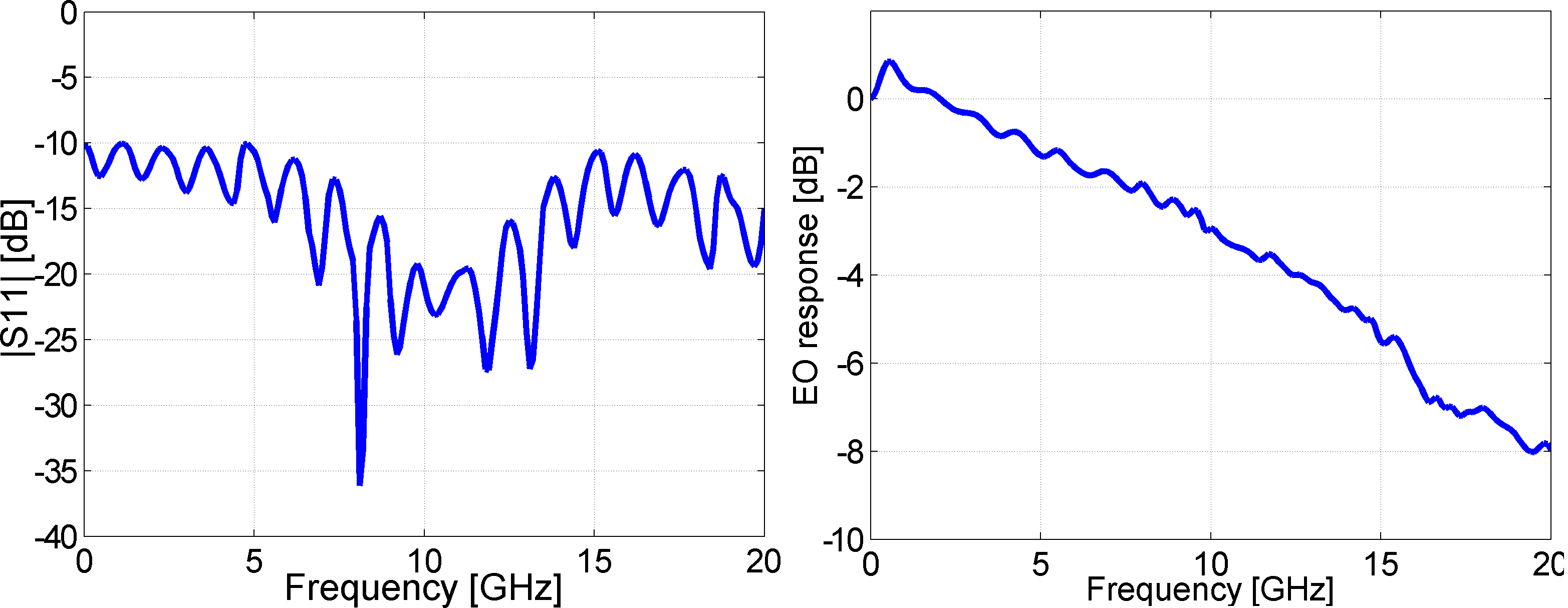
In Fig. 3 we show the microwave reflection coefficient (|S11|) and electro-optic response.
From Fig. 3 one can see that the electrical reflection is always below -10 dB and the 3 dBelectro-optic bandwidth is 10 GHz.
Figure 3. Typical modulator electrical reflection (S11) and electro-optic (EO) response .
The corresponding switching voltage is 2.1 V (measured at 1 kHz). The modulator could
Received 27 Jun 2007; revised 2 Aug 2007; accepted 6 Aug 2007; published 9 Aug 2007
20 August 2007 / Vol. 15, No. 17 / OPTICS EXPRESS 10742
therefore easily be driven with significant extinction by a low-cost driver which typically pro-vides less than 3 V for 10 Gb/s bit rate. When system measurements were carried out with anInphi 1015EA driver (i.e. driver for electro-absorption modulators) and Agilent sampling oscil-loscope (30 GHz optical head) a dynamic extinction of 13.5 dB (typical) was obtained, whichis largely suitable for a 10Gb/s transmitter module. Conclusions
In conclusion we have shown that domain inversion can be used to produce very low-voltageintegrated LiNbO3 modulators that can be driven by cheap electronics. It is also clear thatthe improvement associated with our structure is in the reduction of voltage length product(increase in efficiency); hence DI could also be used to shorten modulators for standard Mach-Zehnder modulator drivers, thus enabling greater integration. Besides driving voltage reductionthe domain-inverted modulator offers several additional advantages with respect to a standardsingle-domain counterparts, including chirp-free operation and higher thermal stability. In thefuture more complex structures can be envisaged with the aim of tailoring the frequency re-sponse of the modulator (longitudinal DI) while still increasing the efficiency (transversal pol-ing as in this work).
Received 27 Jun 2007; revised 2 Aug 2007; accepted 6 Aug 2007; published 9 Aug 2007
20 August 2007 / Vol. 15, No. 17 / OPTICS EXPRESS 10743
The first World Conference on Breast Cancer acknowledged that higher levels of estrogen increased the risk of breast cancer. 27 out of 31 studies have found that even one abortion can increase the risk of developing breast cancer. Having a first child before the age of 18 years reduces the breast cancer risk dramatically. In first trimester miscarriages, the estradiol (estrogen) levels are usua
Continuació de la pàgina anterior La línia de l’AVE facilitarà el transport de mercaderies Pensa vostè que la construcció de la línia de l’AVE de la meva indústria (% respostes) (Barcelona-Madrid, Barcelona-França), facilitarà el transport de mercaderies de la vostra empresa? (empreses industrials) Núm. 5 · Maig de 2007 Aquest Informe s’ha elaborat per
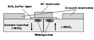 Figure 1. Cross section of proposed domain-inverted LiNbO3 modulator.
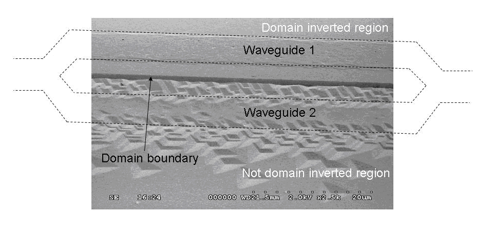
 typically in the 3 to 4 dB range. High-voltage (>10 kV) pulsed poling is performed after Tiindiffusion on the 0.5-mm thick crystal. Figure 2 shows the top (z-) of the LiNbO 3 structurerevealed by etching. The domain-inverted boundary is clearly in the middle of the two Ti indif-fused waveguides which are in opposite-domain regions. In fact the process is now developedfor a 4” wafer with a thickness of 0.5 mm. The uniformity of poling and waveguides over thefull wafer size ensures a high yield (currently 95%) for the overall chip fabrication. Compared
Figure 2. SEM image of etched LiNbO3 structure. The domain boundary lies in betweenthe two Mach-Zehnder waveguides.
typically in the 3 to 4 dB range. High-voltage (>10 kV) pulsed poling is performed after Tiindiffusion on the 0.5-mm thick crystal. Figure 2 shows the top (z-) of the LiNbO 3 structurerevealed by etching. The domain-inverted boundary is clearly in the middle of the two Ti indif-fused waveguides which are in opposite-domain regions. In fact the process is now developedfor a 4” wafer with a thickness of 0.5 mm. The uniformity of poling and waveguides over thefull wafer size ensures a high yield (currently 95%) for the overall chip fabrication. Compared
Figure 2. SEM image of etched LiNbO3 structure. The domain boundary lies in betweenthe two Mach-Zehnder waveguides.